Diagram Of A Pcb
Pcb circuit diagram apk for android download Schematics vs pcb designs Schematic software
Schematic vs. Layout: PCB Geometry, Parasitics, and Signal Integrity
Pcb diagram block state testing operated itself according final crl ece edu Electronic circuit kicad zuken schematic allpcb routing diptrace Pcb multilayer board process flow circuit printed types diagram chart pcba layer flowchart assembly manufacturing different routing electronic components inner
How to convert pcb to schematic diagram?
Difference between schematic diagram and pcb layout : diptraceSchematic pcd instructables Pcb design software – which one is best?Difference between schematic diagram and pcb layout : diptrace.
Mastering the art of pcb design basicsSchematic layout pcb vs parasitics geometry signal integrity board Pcb circuit printed schematics board schematic boards flexible designs vs aluminum altium engineering circuits stackPcb android apkpure winudf wiring.

Schematic convert
Circuits mastering checks protoexpressPcb conditioner Diagram pcb control dan cara pemasangannyaDiagram circuito elettronica schematic stampato basics circuits diagramma lying mastering component sierra protoexpress.
Multilayer pcbMastering the art of pcb design basics Schematic vs. layout: pcb geometry, parasitics, and signal integrity.


Multilayer PCB | Types of PCB | Design, Tutorial, Manufacturing Process

Schematic vs. Layout: PCB Geometry, Parasitics, and Signal Integrity

Schematics vs PCB designs - Electrical Engineering Stack Exchange

Schematic Software - Wiring Diagram

Mastering the Art of PCB Design Basics | Sierra Circuits

PCB Circuit Diagram APK for Android Download

How to Convert PCB to Schematic Diagram? - RAYPCB
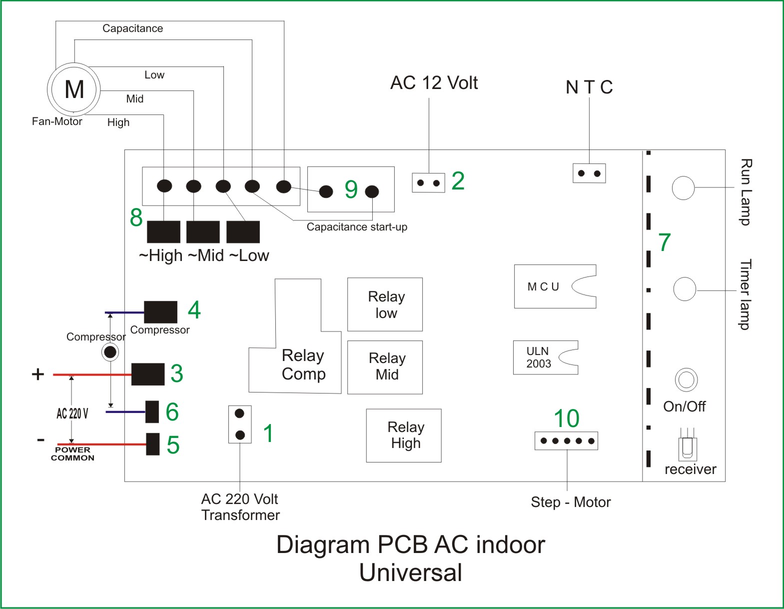
Diagram PCB control dan cara pemasangannya

Mastering the Art of PCB Design Basics | Sierra Circuits

PCB Design Software – Which One is Best? | PREDICTABLE DESIGNS